Macroelectronic Integrated Circuits Using High-Performance Separated Carbon Nanotube Thin-Film Transistors

Application: Transistors

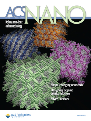
Citation: Chuan Wang, Jialu Zhang, Chongwu Zhou, ACS Nano (2010), 4, 12, 7123–7132.

Summary: Macroelectronic integrated circuits are widely used in applications such as flat panel display and transparent electronics, as well as flexible and stretchable electronics. However, the challenge is to find the channel material that can simultaneously offer low temperature processing, high mobility, transparency, and flexibility. Here in this paper, we report the application of high-performance separated nanotube thin-film transistors for macroelectronic integrated circuits. We have systematically investigated the performance of thin- film transistors using separated nanotubes with 95% and 98% semiconducting nanotubes, and high mobility transistors have been achieved. In addition, we observed that while 95% semiconducting nanotubes are ideal for applications requiring high mobility (up to 67 cm2 V-1 s-1) such as analog and radio frequency applications, 98% semiconducting nanotubes are ideal for applications requiring high on/off ratios (>104 with channel length down to 4µm). Furthermore, integrated logic gates such as inverter, NAND, and NOR have been designed and demonstrated using 98% semiconducting nanotube devices with individual gating, and symmetric input/output behavior is achieved, which is crucial for the cascading of multiple stages of logic blocks and larger scale integration. Our approach can serve as the critical foundation for future nanotube-based thin-film macroelectronics.


Advances in Carbon Nanotube Based Electrochemical Sensors for Bioanalytical Applications

Application: Review Articles

Citation: Sandeep Kumar Vashista, Dan Zhenga, Khalid Al-Rubeaand, John H.T. Luonge and Fwu-Shan Sheu, Biotechnology Advances (2011), 29, 2, 169-188.

Summary: Electrochemical (EC) sensing approaches have exploited the use of carbon nanotubes (CNTs) as electrode materials owing to their unique structures and properties to provide strong electrocatalytic activity with minimal surface fouling. Nanofabrication and device integration technologies have emerged along with significant advances in the synthesis, purification, conjugation and biofunctionalization of CNTs. Such combined efforts have contributed towards the rapid development of CNT-based sensors for a plethora of important analytes with improved detection sensitivity and selectivity. The use of CNTs opens an opportunity for the direct electron transfer between the enzyme and the active electrode area. Of particular interest are also excellent electrocatalytic activities of CNTs on the redox reaction of hydrogen peroxide and nicotinamide adenine dinucleotide, two major by-products of enzymatic reactions. This excellent electrocatalysis holds a promising future for the simple design and implementation of on-site biosensors for oxidases and dehydrogenases with enhanced selectivity. To date, the use of an anti-interference layer or an artificial electron mediator is critically needed to circumvent unwanted endogenous electroactive species. Such interfering species are effectively suppressed by using CNT based electrodes since the oxidation of NADH, thiols, hydrogen peroxide, etc. by CNTs can be performed at low potentials. Nevertheless, the major future challenges for the development of CNT-EC sensors include miniaturization, optimization and simplification of the procedure for fabricating CNT based electrodes with minimal non-specific binding, high sensitivity and rapid response followed by their extensive validation using “real world” samples. A high resistance to electrode fouling and selectivity are the two key pending issues for the application of CNT-based biosensors in clinical chemistry, food quality and control, waste water treatment and bioprocessing.

Fundamental Limits on the Mobility of Nanotube-Based Semiconducting Inks

Application: Transistors

Citation: Nima Rouhi, Dheeraj Jain, Katayoun Zand, Peter John Burke, Advanced Materials (2011), 23, 1, 94-99.

Summary: High mobility and high on/off ratio thin-film transistors are fabricated using solution-based deposition of purified semiconducting carbon nanotubes. A comprehensive spectrum of the density starting from less than 10 tubes μm-2 to the high end of around 100 tubes μm-2 is investigated. This study provides the first important roadmap for the tradeoffs between mobility and on/off ratio in nanotube-based semiconducting inks.

Exploring the Physicoelectrochemical Properties of Graphene

Application: Other Research

Citation: Dimitrios K. Kampouris and Craig E. Banks, Chemistry Communications (2010), 46, 47, 8865-9068.

Summary: Convincing evidence is presented demonstrating that the electro-catalytic nature of graphene resides in electron transfer from the edge of graphene which structurally resembles the behaviour of edge plane (rather than basal plane) of highly ordered pyrolytic graphite. The impact of surfactants intrinsic to graphene on the electrochemical response is highlighted.

Ultrabroadband Photodetection Based on Graphene Ink

Application: Optoelectronic Devices

Citation: A. Radoi, A. Iordanescu, A. Cismaru, M. Dragoman, D. Dragoman, Nanotechnology (2010), 21 455202.

Summary: We report photodetection in a very large spectral bandwidth, which encompasses ultraviolet, visible and near infrared, using graphene inks or graphene inks functionalized with either gold or silver nanoparticles, or gold nanoparticles further encapsulated with bovine serum albumin deposited on interdigitated electrodes fabricated on a silicon dioxide/silicon substrate. In contrast to gold-functionalized graphene inks, which have responsivities better than 1 mA W-1 at a 0.1 V bias over the huge bandwidth extending from 215 to 2500 nm, Ag-functionalized inks show at least a four-fold increased responsivity, with a record value of 13.7 mA W-1 in near infrared.

The Electrochemical Response of Graphene Sheets is Independent of the Number of Layers from a Single Graphene Sheet to Multilayer Stacked Graphene Platelets

Application: Electrochemical

Citation: Madeline Shuhua Goh, Martin Pumera, Chemistry – An Asian Journal (2010), 5, 11, 2355–2357.

Summary: We compare electrochemical response of single-, few-, and multilayer graphene sheets and conclude that there is no significant difference between them. Therefore, there is no need for single-layer graphene sheets for electrochemical applications because multilayer graphene provides equal voltammetric performance.

Tip-Enhanced Raman Spectroscopic Imaging of Localized Defects in Carbon Nanotubes

Application: Other Research

Citation: Carsten Georgi, Achim Hartschuh, Applied Physics Letters (2010), 97, 143117.

Summary: We used tip-enhanced Raman spectroscopy to study defect induced D-band Raman scattering in metallic single-walled carbon nanotubes with a spatial resolution of 15 nm. The spatial extent of the D-band signal in the vicinity of localized defects is visualized and found to be about 2 nm only. Using the strong optical fields underneath the tip, we photogenerate localized defects and derive a relation between defect density and resulting D-band intensity.

Flexible, Transparent Single-Walled Carbon Nanotube Transistors with Graphene Electrodes

Application: Transistors

Citation: Sukjae Jang, Houk Jang, Youngbin Lee, Daewoo Suh, Seunghyun Baik, Byung Hee Hong, Jong-Hyun Ahn, Nanotechnology (2010), 21 425201.

Summary: This paper reports a mechanically flexible, transparent thin film transistor that uses graphene as a conducting electrode and single-walled carbon nanotubes (SWNTs) as a semiconducting channel. These SWNTs and graphene films were printed on flexible plastic substrates using a printing method. The resulting devices exhibited a mobility of ~ 2 cm2 V -1 s -1, On/Off ratio of ~ 102, transmittance of ~ 81% and excellent mechanical bendability.

Characterization of Carbon Nanotube Nanoswitches with Gigahertz Resonance Frequency and Low Pull-In Voltages Using Electrostatic Force Microscopy

Application: Electromechanical

Citation: Miao Lu, Xuekun Lu, Min-Woo Jang, Stephen A. Campbell, Tianhong Cui, Journal of Micromechanics and Microengineering (2010), 20, 105016.

Summary: An electrostatic force microscope (EFM) was used to characterize single-walled carbon nanotube (SWNT)-based nanoswitches in this paper. A conductive atomic force microscopy (AFM) tip acted as a mechanical probe as well as a positioning electrode in the experiment. The resonance frequency of the SWNT beams was computed from the measured SWNTs’ dimension and spring constant. The pull-in voltages and the corresponding gaps were extracted simultaneously from a set of force curves at different EFM probe bias voltages. The adhesive force between the AFM tip and the SWNT beam was measured through the analysis of retract force curves. The relationship between the pull-in voltage and the SWNT nanoswitch gap was in agreement with the electrostatic pull-in theory. Long-range forces such as meniscus force or electrostatic force from surface charges engaged the SWNT beam when the gap was below 6 nm in atmosphere. The SWNT beam with a resonance frequency of 1.1 GHz was actuated by a voltage of 2 V for a gap of 6.5 nm. The average adhesive force between an SWNT beam and a platinum/iridium (PtIr5)-coated tip was found to be about 50 nN. Considering the stiffness of the 1.1 GHz SWNT beam, the elastic restoring force at 6.5 nm exceeds 53 nN, which will overcome the adhesive force and release the 1.1 GHz SWNT beam. Finally, some possible approaches to further improve the behavior of SWNT nanoswitches are discussed.

Electronic-Structure-Dependent Bacterial Cytotoxicity of Single-Walled Carbon Nanotubes

Application: Biomedical

Citation: Chad D. Vecitis, Katherine R. Zodrow, Seoktae Kang, Menachem Elimelech, ACS Nano (2010), 4, 9, 5471-5479.

Summary: Single-walled carbon nanotubes (SWNTs) have been previously observed to be strong antimicrobial agents, and SWNT coatings can significantly reduce biofilm formation. However, the SWNT antimicrobial mechanism is not fully understood. Previous studies on SWNT cytotoxicity have concluded that membrane stress (i.e., direct SWN–bacteria contact resulting in membrane perturbation and the release of intracellular contents) was the primary cause of cell death. Gene expression studies have indicated oxidative stress may be active, as well. Here, it is demonstrated for the first time how SWNT electronic structure (i.e., metallic versus semiconducting) is a key factor regulating SWNT antimicrobial activity. Experiments were performed with well-characterized SWNTs of similar length and diameter but varying fraction of metallic nanotubes. Loss of Escherichia coli viability was observed to increase with an increasing fraction of metallic SWNTs. Time-dependent cytotoxicity measurements indicated that in all cases the majority of the SWNT antimicrobial action occurs shortly after (<15 min) bacteria–SWNT contact. The SWNT toxicity mechanism was investigated by in vitro SWNT-mediated oxidation of glutathione, a common intracellular thiol that serves as an antioxidant and redox state mediator. The extent of glutathione oxidation was observed to increase with increasing fraction of metallic SWNTs, indicating an elevated role of oxidative stress. Scanning electron microscopy images of E. coli in contact with the SWNTs demonstrated electronic structure-dependent morphological changes consistent with cytotoxicity and glutathione oxidation results. A three-step SWNT antimicrobial mechanism is proposed involving (i) initial SWN–bacteria contact, (ii) perturbation of the cell membrane, and (iii) electronic structure-dependent bacterial oxidation.

Ultrasensitive Detection of DNA Molecules with High On/Off Single-Walled Carbon Nanotube Network

Citation: Dongliang Fu, Haruya Okimoto, Chun Wei Lee, Taishi Takenobu, Yoshihiro Iwasa, Hiromichi Kataura, Lain-Jong Li, Advanced Materials (2010), 10.1002/adma.201002305.

Summary: Semiconducting networks were found to be extremely sensitive to charges, which promises the electrical detection of ultralow concentrations of DNA (down to 0.1 fM, ∼100 DNA molecules).

Micro Tactile Sensors with a Suspended and Oriented Single Walled Carbon Nanotube Beam Embedded in Polydimethylsiloxane Elastomer

Application: Other Research

Citation: Miao Lu, Dongjin Lee, Taiho Yeom, Tianhong Cui, Sensor Letters (2010), 8, 4, 639-644.

Summary:A tactile sensor utilizing a patterned, aligned, and suspended SWNT film as a sensing element is reported in this paper. The sensor was prepared on both silicon and polymer substrates to expand its potential applications to different working conditions. First, a trench 10 μm deep with Cr/Au electrodes on both sides of the trench was realized. Next, dense and oriented SWNT films were self-assembled using dielectrophoresis through in-situ control of the dc resistance of the film. Follow that, the SWNT film was patterned by lithography and oxygen plasma etching to prepare a suspended SWNT beam. Finally, PDMS primer was spin-coated on the structure and cured to protect the SWNT beam and realize a robust tactile sensor. In nanoindentation test, a piezoresistive sensitivity of 5%/mN and a detection limitation of 2 μN were demonstrated. This simple and low temperature fabrication technology is believed to be very promising for flexible tactile sensor and sensor array in applications to smart robots, implantable clinic tools, or embedded pressure sensors in micro fluidic systems.

Challenges in the Use of 1D Nanostructures for On-chip Biosensing and Diagnostics: A Review

Application: Review Articles

Citation: Kannan Balasubramanian, Biosensors and Bioelectronics (2010), 26, 4, 1195-1204.

Summary: This review outlines the use of one-dimensional nanostructures (1D-NS) for the detection of biomolecules on a chip. The materials discussed here include carbon nanotubes, metallic and semiconducting nanowires and nanochannels. While nanotubes and naowires have predominantly been used as electrical detectors, nanochannels are promising frameworks for optical detection in applications such as separation, preconcentration and DNA mapping. The primary expectation for all the three types of 1D-NS lies in the promise for ultimate single molecule detection. Furthermore, the electrical double layer governs the physics behind biosensing in all the three systems. The review starts by shedding light on the advantages arising due to the use of 1D nanostructures, followed by a discussion of fundamental aspects such as double layer effects and sensing methodologies. After this, the three kinds of 1D-NS are introduced. The main focus of the review is an in-depth analysis of the current achievements in the field and the major challenges that are to be overcome for the widespread use of such nanostructures in applications such as lab-on-a-chip devices and point-of-care diagnostics.

A Generalized Method for Evaluating the Metallic-to-Semiconducting Ratio of Separated Single-Walled Carbon Nanotubes by UV−vis−NIR Characterization

Application: Other Research

Citation: Liping Huang, Hongliang Zhang, Bin Wu, Yunqi Liu, Dacheng Wei, Jianyi Chen, Yunzhou Xue, Gui Yu, Hisashi Kajiura, Yongming Li, The Journal of Physical Chemistry (2010), 114, 28, 12095–12098.

Summary:A general and useful method has been developed to evaluate the metallic-to-semiconducting (M/S) ratio for separated single-walled carbon nanotubes (SWNTs). By virtue of measuring UV−vis−NIR spectra of a variety of solutions with different ratios of metallic-rich to semiconducting-rich SWNTs, the commercial IsoNanotubes samples as well as metallic-rich HiPCO SWNTs (HiPCO-M) separated by an Agarose gel method have been evaluated. Values of 99.5% metallic contents for IsoNanotubes-M, 98.9% semiconducting contents for IsoNanotubes-S, and 1.24 for the absorption coefficient of IsoNanotubes, whereas 80.4% metallic contents for HiPCO-M and 1.05 for the absorption coefficient of HiPCO SWNTs were obtained. This method does not need pure metallic (M-) or semiconducting (S-) SWNTs as references. Furthermore, we found that this method can also be applied to evaluate the M/S ratio for any SWNT samples.

Evaluating Defects in Solution-Processed Carbon Nanotube Devices via Low-Temperature Transport Spectroscopy

Application: Review Articles

Citation: Paul Stokes and Saiful I. Khondaker, ACS Nano (2010), 4, 5, 2659–2666.

Summary: We performed low-temperature electron transport spectroscopy to evaluate defects in individual single-walled carbon nanotube (SWNT) devices assembled via dielectrophoresis from a surfactant-free solution. At 4.2 K, the majority of the devices show periodic and well-defined Coulomb diamonds near zero gate voltage corresponding to transport through a single quantum dot, while at higher gate voltages, beating behavior is observed due to small potential fluctuations induced by the substrate. The Coulomb diamonds were further modeled using a single electron transistor simulator. Our study suggests that SWNTs derived from stable solutions in this work are free from hard defects and are relatively clean. Our observations have strong implications on the use of solution-processed SWNTs for future nanoelectronic device applications.

Evaluation of Transparent Carbon Nanotube Networks of Homogeneous Electronic Type

Application: Other Research

Citation: Roderick K. Jackson, Andrea Munro, Kenneth Nebesny, Neal Armstrong, Samuel Graham, ACS Nano (2010), 4, 3, 1377-1384.

Summary: In this report, we present a description of the optical and electronic properties of as-deposited, annealed, and chemically treated single-walled carbon nanotube (SWNT) films showing metallic or semiconducting behavior. As-deposited and annealed semiconducting SWNT films were significantly less conductive than metallic SWNT films; however, chemical treatment of semiconducting SWNT films resulted in sheet resistance values as low as 60 Ω·sq−1 in comparison to 76 Ω·sq−1 for similarly processed metallic SWNT films. We conclude that the greater improvement of electrical conductivity observed in the semiconducting SWNT film results from the difference in the density of available electronic states between metallic and semiconducting SWNTs. A corroborative investigation of the change in surface work function and the chemical composition of SWNT films, as revealed by X-ray photoelectron spectroscopy, is provided to support these conclusions and to give new perspective to the formation of electronically homogeneous SWNT networks.

Enhanced Electromodulation of Infrared Transmittance in Semitransparent Films of Large Diameter Semiconducting Single-Walled Carbon Nanotubes

Application: Optoelectronic Devices

Citation: Feihu Wang, Mikhail E. Itkis, Robert C. Haddon, Nano Letters (2010), 10, 3, 937-942.

Summary: We report a comprehensive study of the gate-induced electromodulated transmittance of infrared light by single-walled carbon nanotube (SWNT) thin films. The observed electromodulation is significantly enhanced by utilizing large diameter SWNTs, increasing the ratio of semiconducting to metal SWNTs, and by decreasing the SWNT film thickness. The amplitude of the effect reported herein (∼7%) is more than an order of magnitude larger than in previous SWNT thin film solid state devices.

Memory Effect of a Single-Walled Carbon Nanotube on Nitride-Oxide Structure Under Various Bias Conditions

Application: Other Research

Citation: Hongsik Park, Hyunjung Shin, Jin Ho Kim, Seungbum Hong, Jimmy Xu, Applied Physics Letters (2010) 96, 023101.

Summary: We report on the memory effect of single-walled carbon nanotubes (SWNTs (placed on a nitride-oxide layer structure designed as a charge storage medium. The conductance of the SWNT was modulated by the injected charge in the nitride-oxide interface and the polarities of injected charges were then detected. A large on/off-state current ratio ≶104(was obtained at a small program/erase voltage range ≶3 V(. We also studied the effect of a half-selected cell on the conductance of the SWNTs to identify the issues with cross-point memory architecture.

Electrochemical Analysis of Single-Walled Carbon Nanotubes Functionalized with Pyrene-Pendant Transition Metal Complexes

Citation: Eden W. McQueen, Jonas I. Goldsmith, JACS (2009), 131, 48, 17554-17556.

Summary: The noncovalent functionalization of single-walled carbon nanotubes (SWNTs) is important in the development of advanced materials and nanoelectronic sensors and devices. A cobalt-terpyridine transition metal complex with pendant pyrene moieties has been shown to successfully functionalize SWNTs via noncovalent π−π stacking interactions. Cyclic voltammetry at SWNT coated platinum electrodes has been utilized to investigate the process of surface modification and provides conclusive evidence of robust surface functionalization. The electrochemical methodology for examining surface functionalization of SWNTs described herein is generalizable to any redox-active system and provides a simple and powerful means for in situ examination of processes occurring at the surface of nanostructured materials.

Wafer-Scale Fabrication of Separated Carbon Nanotube Thin-Film Transistors for Display Applications

Application: Transistors

Citation: Chuan Wang, Jialu Zhang, Koungmin Ryu, Alexander Badmaev, Lewis Gomez De Arco, Chongwu Zhou, Nano Letters (2009), 9, 12, 4285-4291.

Summary: This paper demonstrates a functioning OLED display device based on a waferscale
assembly of carbon nanotube thinfilm transistors. Using IsoNanotubes S 95%, the University of California produced transistors with high yield (>98%), low sheet resistance (25kΩ/sq), high current density ( 10µA/µm), and superior mobility (52 cm 2 V-1s-1). Moreover, on/off rations of >10^4 were achieved in devices with channel length L>20µm. To the best of our knowledge, these are the best concurrent CNT transistor numbers reported in the literature to date.

80 GHz Field-Effect Transistors Produced Using High Purity Semiconducting Single-Walled Carbon Nanotubes

Application: Transistors

Citation: L. Nougaret, H. Happy, G. Dambrine, V. Derycke, J. -P. Bourgoin, A. A. Green, M. C. Hersam, Applied Physics Letters (2009) 94, 243505.

Summary: In this study, solutions of 99% pure semiconducting nanotubes were used to fabricate SWNT field-effect transistors (FETs) with extrinsic and intrinsic current gain cutoff frequencies of ~15 and ~80 GHz, respectively. Importantly, this study also demonstrates that precise nanotube alignment is not required to achieve excellent performance in high-frequency devices.

Thin Film Nanotube Transistors Based on Self-Assembled, Aligned Semiconducting Carbon Nanotube Arrays

Application: Transistors

Citation: Michael Engel, Joshua P. Small, Mathias Steiner, Marcus Freitag, Alexander A. Green, Mark C. Hersam, Phaedon Avouris, ACS Nano (2008), 2, 12, 2445–2452.

Summary: The IBM T.J. Watson Research Center with Northwestern University fabricated thin-film transistors (TFTs) from DGU produced semiconducting CNTs. To confirm the semiconducting purity of the CNTs, the team synthesized 83 single nanotube transistors from the same DGU produced source material. 82 of the 83 transistors were found to contain a semiconducting nanotube, empirically confirming the material’s calculated level (99%) of semiconducting enrichment.

Progress Towards Monodisperse Single-Walled Carbon Nanotubes

Application: Review Articles

Citation: Mark C. Hersam, Nature Nanotechnology (2008) 3, 387-394.

Summary: This paper discusses the advantages of DGU over other nanotube sorting strategies, such as dielectrophoresis, selective chemistry, controlled electrical breakdown, and chromatography. In brief, the principle advantages of DGU are its:

  • Demonstrated scalability
  • Compatibility with a wide range of starting materials
  • Use of reversible functionalization chemistry
  • Iterative repeatability