 Semiconducting carbon nanotubes may replace or complement traditional semiconductors in both high-performance and low-cost thin film transistor (TFT) devices. Today, TFTs are most commonly used in the backplanes of LCD and OLED displays. As the flexible electronics industry matures, TFTs will likely be incorporated into a much wider range of commercial electronics.
Demonstrated Results Using Sorted Nanotubes
IBM and the University of Southern California have used our IsoNanotubes-S carbon nanotubes to create TFTs with the best concurrent on/off ratios and on-drive currents reported in the literature to date. (Steiner, M. et. al., Appl. Phys. Lett., (2012), 101, 053123, 4pages)(Wang, C. et. al., Nano Letters, (2009), 9, 12, 4285-4291) (Engel, M., et al., ACS Nano, (2008), 2, 2445-2452)
When used as a local back gate our high-density single walled carbon nanotube thin films were used as an effective Field-Effect Transistor when on an amino-silane-treated hafnium oxide (HfOX) surface (Narasimhamurthy et al., Semiconductor Science and Technology (2011), 26, 075002).
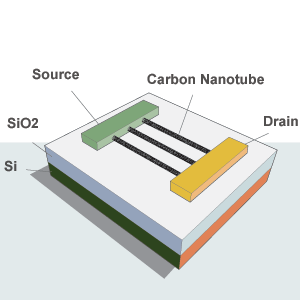
Field-effect transistors (FETs) are the basic building blocks of modern electronics. For decades, FETs have been built using semiconductors like silicon and gallium arsenide as active channel materials.
These materials, however, are subject to well-established performance and processing limitations. Semiconducting carbon nanotubes are ideally suited to replace or complement traditional semiconductors in both high-performance and low-cost FET devices.
Carbon Nanotube Advantages
- Incredible Mobilities: Semiconducting CNTs have been demonstrated to exhibit greater charge carrier mobilities than crystalline silicon (~100,000 cm2/ V•s).
- High Cut-Off Frequencies: Highly separated (99.6% pure) semiconducting CNTs on a fully scalable device platform have achieved the highest experimental values for Intrinsic Current Gain Cut-Off Frequencies (153GHz) and Intrinsic Power Gain Cut-Off Frequencies (30GHz).
- Processability: Carbon nanotubes can be readily dispersed in a number of organic and inorganic solvents. Such dispersions can be printed—via ink-jet or roll-to-roll processes—onto substrates such as glass and plastic.
- Low Schottky Barriers: Large-diameter semiconducting CNTs give rise to small Schottky barriers when used in conjunction with standard source/drain electrode materials, like platinum, titanium, and aluminum.
- Bandgap Tunability: DGU can be used to sort carbon nanotubes by diameter and bandgap. We have the capacity to generate nanotubes that are monodisperse in bandgap from approximately 0.6 to 1.4 eV.